Printed Circuit Board layout is a necessary stage to turn an approved electrical schematic into a producible physical layout: component placement, trace routing, stack-up definition and verification of mechanical and electrical constraints. It is a delicate step of the whole development process, because the choices made at this stage directly affect signal integrity, electromagnetic compatibility, cost and manufacturability.
At Protech we use professional CAD tools such as Altium Designer and Cadence OrCAD/Allegro to manage projects ranging from a single prototype to series production, on single/double-sided, multilayer and rigid-flex boards.

Every layout goes through DRC (Design Rule Check) and DFM (Design for Manufacturability) checks before release to production, to minimize rework, scrap and delays during industrialization.
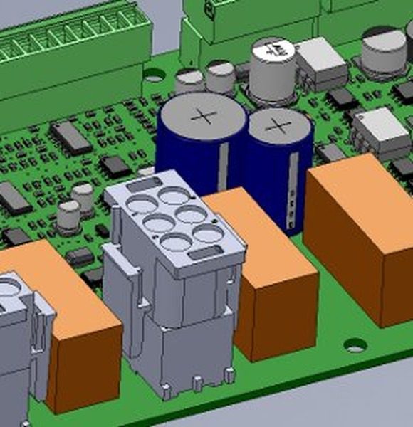
We support you through every stage of mastering, from schematic to production file
We define the stack-up best suited to the application, balancing layer count, dielectric thicknesses and reference planes to guarantee controlled impedance on critical lines. We assess crosstalk, return current paths and electromagnetic compatibility already at the layout stage, to reduce the risk of issues during EMC validation.
Component placement takes into account mechanical, thermal and manufacturability constraints, as well as electrical requirements. Trace routing follows the design rules (DRC) defined for the chosen production process, with attention to thermal vias, ground/power planes and the management of interference between analog, digital and power circuits on the same board.
Before release we verify the manufacturability of the design (DFM/DFA) together with PCB fabricators and assemblers, to align the layout with their processes. The production package includes Gerber RS-274X files, NC drill files, pick and place files, bill of materials (BOM) and assembly documentation.
The stages of our mastering service, from data acquisition to the production file
We import the netlist supplied by the customer, or generate it from the electrical schematic, checking its consistency with the design and matching the chosen components to their footprints.
We build and maintain component libraries to the customer's specifications, acquiring the board outline or the mechanical drawing in DXF format as a reference for the layout.
We set the layout design rules and define the stack-up best suited to the application, based on layer count, dielectric thicknesses and impedance constraints.
We place components on the board taking into account electrical, thermal, mechanical and manufacturability constraints, in preparation for the following routing stages.
We define the electrical parameters of power and high-speed signal lines, using routing techniques for differential pairs, length-matching and crosstalk protection; we complete the routing and place the in-circuit test points requested by the customer.
We generate Gerber files, pick and place files and all the documentation needed for production, together with 3D mechanical files in STEP format to check the fit with the mechanical design.
Protech s.a.s. di Girardi A. & c.
Registered Office: Via dei Pini 21, 31033 - CASTELFRANCO VENETO (TV) - Italy
VAT/Tax ID 03510960267 - SDI Code WP7SE2Q
info@protechgroup.it
© 2000-2026 Protech Engineering. All rights reserved · Privacy Policy